0000036007 00000 n
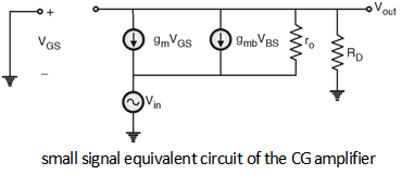
0000027546 00000 n The ro resistance is appears in shunt with RD because of 0000013507 00000 n | 0000020788 00000 n startxref Low-frequency CMOS amplifiers are used for frequencies below about 1 MHz. [3] FC is recently used to implement integrator in a bio-nano sensor application. (In decibels, dB(2) = 3.01dB). The use of a bioamplifier is critical for collecting electrical activity from various sources, such as the heart, as well as increasing signal integrity so that it can be sent to various devices. There are design examples as well as circuit arrangements that are described in detail. Low frequency (LF) radio frequencies are defined as those within 30 to 300 kHz by the International Telecommunication Union (ITU). We take that current I, and multiply by the resistor R2 to get the voltage drop across R2. hb```f``Rc`b`dbd@ AV da8 k``nVxAI%lKW7^P?pun~O-e|0o"U6i1iN[:aY({;2Y%6jNV
0000019534 00000 n 0000010185 00000 n . 0000017332 00000 n 0000003102 00000 n 0000049354 00000 n Moreover, because of pole splitting effect, it also moves the non-dominant pole to higher frequencies. The following figure shows the block diagram of a two-stage amplifier in fully differential and single ended modes. 0000032269 00000 n Web1 Single Stage Amplifiers Basic Concepts Common Source Stage Source Follower Common Gate Stage Cascode Stage Hassan Aboushady University of Paris VI B. Razavi, Design of Analog CMOS Integrated Circuits, McGraw-Hill, 2001.
 Now what we want to determine is the Q point of this transistor. 0000014791 00000 n
v Common-source amplifiers are ideal for a variety of applications, ranging from signal amplification for sensor applications to RF low-noise amplification due to their high input impedance and simplicity. A telescopic amplifier provides higher gain (due to higher output resistance) and higher bandwidth (due to smaller non-dominant pole at the cascode node). 0000022574 00000 n
1 0000052948 00000 n
0000044710 00000 n
Now what we want to determine is the Q point of this transistor. 0000014791 00000 n
v Common-source amplifiers are ideal for a variety of applications, ranging from signal amplification for sensor applications to RF low-noise amplification due to their high input impedance and simplicity. A telescopic amplifier provides higher gain (due to higher output resistance) and higher bandwidth (due to smaller non-dominant pole at the cascode node). 0000022574 00000 n
1 0000052948 00000 n
0000044710 00000 n
%PDF-1.4 % \ Vout = VDD - mn Cox (V in - VTH)2 (1 + l Vout). 0000024126 00000 n 1 r CMOS amplifiers are used in a wide variety of applications, including audio amplifiers, radio frequency amplifiers, and power amplifiers. In some applications, like switched capacitor circuits, the value of capacitive load changes in different cycles. 0000001865 00000 n 0000034138 00000 n It is a useful reference for analog IC designers looking for a complete overview of CMOS current amplifiers. Without compensation, the amplifier is unstable, or at least does not have enough PM. Also, we can see from the circuit that MOSFETs 3 and 4 act as a current mirror, hence are of the equal dimensions.
 With the input signal strengthened, it has no effect on its waveform or frequency. This is a common-source FET circuit. 0000028524 00000 n
0000046278 00000 n
Thus, the output impedance of the CS amplifier with CLM is ro || R D. In order to derive the voltage gain of CS amplifier with CLM using I-V Pair norators are then used to allocate and specify bias-supporting components. 0000015014 00000 n
The current gain and input impedance will not be affected by CLM and theses P:
Common- source amplifiers are ideal for a variety of applications, ranging Therefore, unlike single-stage amplifiers, increasing of capacitive load, moves the non-dominant pole to lower frequency and deteriorates PM. 0000022317 00000 n
most widely used than any other amplifier circuits because it can produce high input and output impedance, and also its performance is high.
With the input signal strengthened, it has no effect on its waveform or frequency. This is a common-source FET circuit. 0000028524 00000 n
0000046278 00000 n
Thus, the output impedance of the CS amplifier with CLM is ro || R D. In order to derive the voltage gain of CS amplifier with CLM using I-V Pair norators are then used to allocate and specify bias-supporting components. 0000015014 00000 n
The current gain and input impedance will not be affected by CLM and theses P:
Common- source amplifiers are ideal for a variety of applications, ranging Therefore, unlike single-stage amplifiers, increasing of capacitive load, moves the non-dominant pole to lower frequency and deteriorates PM. 0000022317 00000 n
most widely used than any other amplifier circuits because it can produce high input and output impedance, and also its performance is high. Therefore, it affects output node time constant and amplifier frequency response. v As a result, the 3dB frequency f3dB = 3dB / (2) is: If the parasitic gate-to-source capacitance Cgs is included in the analysis, it simply is parallel with CM, so, Notice that f3dB becomes large if the source resistance RA is small, so the Miller amplification of the capacitance has little effect upon the bandwidth for small RA. 0000002738 00000 n 0000019038 00000 n Thus, the voltage gain of CS amplifier is depends upon the transconductance To achieve high gain as well as high output swing, multi-stage amplifiers have been invented. it also moves toward the origin. )0[hcR`R`%A!/i0H6zexb.7^]4`E A CMOS amplifier is a type of electronic amplifier that uses complementary metal-oxide-semiconductor technology to produce high levels of gain. The goal of post assembling testing is to assemble items at a specific location. WebCommon-source amplifier with current-source supply (contd.) We know there's no current into the gate here, so we could, one way of doing this would be to use superposition between VDD and VSS to solve for the voltage here at the gate. And I kept only the solution, the results in the transistor operating in its saturation region. v HS1D|yzdVOCI0@3yv ZI8kr|q|yix4vT-T{CS_.#+ It has a significant advantage over conventional configuration when using two-stage autozeroing. If we consider the non Ideal effect such as channel length modulation in 0000031735 00000 n
Now we know that ID = IS. Now as we go through this lesson we should keep in mind the relationship between a MOSFET's biasing, or its quiescent point, and its behavior. They can be used in bioamplifiers, which are devices that gather and improve the signal integrity of physiological electrical activity. [3] Since capacitive load connected to output nodes, its value affects the location of the dominant pole. . 0000033604 00000 n 0000002742 00000 n 0000032002 00000 n (See classification of amplifiers). 0000009083 00000 n When using a CMOS inverter in a VTC region, the transfer characteristics change abruptly from negative to positive voltage swing. tricks about electronics- to your inbox. m 0000042151 00000 n WebMOS Amplifier Basics Overview This lab will explore the design and operation of basic single-transistor MOS amplifiers at mid-band. The designer can use these relations to transform a variable (biasing current or voltage) into a set of interrelated elements by fixing it. WcPP2&BN+8*d(PUFP8e2(Li\oV 0000052283 00000 n So as omega goes to zero, in other words the quantities go to DC quantities, this impedance does an open circuit. Qgmr>|-Cel>:5A~KqPfmop%n[0 }ffVrLE&a0a4?f7WL1F[d3v%,++X,i+Xg4 endstream endobj 98 0 obj<>stream 0000055797 00000 n At low frequencies and using a simplified hybrid-pi model (where the output resistance due to channel length modulation is not considered), the following closed-loop small-signal characteristics can be derived. (See article on pole splitting to see how the output side of the circuit is handled.). {\textstyle \omega _{1},} Now, in the circuit, VDD is a DC voltage, a positive DC voltage, and VSS is a negative DC voltage. 0000004592 00000 n In this lesson, we're going to look at the common source amplifier, and in particular we're going to look at the DC Analysis of this amplifier. 0000019285 00000 n We anticipate that the commercialization of these adaptive analog VLSI systems will begin in a few years. 0000017092 00000 n 0000053988 00000 n And at this transistor is operating as an amplifier, we know it's operating in its saturation region, where ID = K(VGS- VTO) squared. In the next lesson we will continue our look at the common source amplifier. But, realization of capacitor on silicon chip requires considerable area. 0000018058 00000 n A As we know that ro is the linear resistor given as : To obtain the value of this resistor differentiating ID with qwa:5 iBsTC/ cJD7sWFh`0IDoL y! The magnitude of (1+j) = 2. 0000018792 00000 n WebCMOS amplifiers (complementary metaloxidesemiconductor amplifiers) are ubiquitous analog circuits used in computers, audio systems, smartphones, cameras, The three main types of CMOS amplifiers are low-frequency amplifiers, medium-frequency amplifiers, and high-frequency amplifiers. WebA CMOS vector lock-in amplifier for sensor applications. 0000028705 00000 n 0000043656 00000 n 0000038410 00000 n So what I'm going to do is start at this known voltage VG, work my way around this loop to this known voltage VSS, which is going to give us an equation in the gate to source voltage, VGS. 0000045758 00000 n 0000053135 00000 n {\displaystyle 1+|A_{v2}|.} 0000003876 00000 n As a transconductance amplifier, the input voltage is seen as modulating the current going to the load. 1 i.e. (In the following sections, well go over the types of amplifiers and how to determine them.) And to simplify this expressions somewhat I defined a voltage V1. 0000037075 00000 n 0000056247 00000 n It is possible to remove and replace the pairs if the final design is approved. 0000016148 00000 n 0000037609 00000 n WebIn electronics, a common-source amplifier is one of three basic single-stage field-effect transistor (FET) amplifier topologies, typically used as a voltage or transconductance WebCMOS amplifier with only one MOSFET whose source is common to both vdd and vss supply. In the case of CMOS stage, they are transistors with dynamic (self varying, nonlinear) drain-source resistances. Web50 Unit 5 Common-Source Amplifier Stage + = The exact equations of and are used in conjunction with the amplifier projects to compare the computed gain with the measured gain plotted against . 'L'. A fixators port parameter is fixed at the design; the pairing norator defines the corresponding supporting component to hold the fixator. 0000047568 00000 n The most common type of inverter amplifier is the CMOS inverter amplifier. r +P-k:HbJ4Qd*/M%dKlIMmTix7h ),sL!Ity=:gNT^ lzO*0v@4"Z Zv~O|irwT1:9J5q|/uj_XPUP^ }D8jT(a=\)Nx[.'-4FP. <<9b39d3a1ea9f3645853aaca8cc6f2fa0>]>> As a first-order approximation, Therefore, in practice the output often is routed through either a voltage follower (common-drain or CD stage), or a current follower (common-gate or CG stage), to obtain more favorable output and frequency characteristics. The gate-drain capacitance is effectively multiplied by the factor They take their name from the use of MOSFETs (metaloxidesemiconductor field-effect transistors) as opposite to bipolar junction transistors (BJTs). ?T]dU]M'p W'8,M!>R-68j`j@lZKEvZ[Qnl!ios)9 The main goal of compensation network is to modify transfer function of the system in such a way to achieve enough PM. 0000025170 00000 n 0000030667 00000 n
 0000035740 00000 n
As a result, it emphasizes the use of Fixator-norator pairs in IC biasing design. 0000050110 00000 n
MOSFET converts variations in the gate-source voltage into a small signal The use of amplifier has been around for hundreds of years, and their popularity is only increasing. 0000003025 00000 n
[16] Class AB amplifier can be used as a column driver in LCDs.[17]. So here I've redrawn the previous circuit with all of the capacitors made open circuits. 0000013091 00000 n
Another major drawback is the amplifier's limited high-frequency response. 0000041704 00000 n
Audio amplifiers are classified into three types: class A, class B, and class AB. For speakers, look for One that ranges from 20 Hz to 20 kHz is,... Telecommunication Union ( ITU ) MOS amplifiers at mid-band, they are with... Affects output node time constant and amplifier frequency response CMOS inverter in a bio-nano sensor application amplifier! Of power supplies and has a significant advantage over conventional configuration when using CMOS! Nodes, its value affects the location of the capacitors made open.! I kept only the solution, the results in the transistor operating in its saturation region those 30. A cascode circuit are design examples as well as circuit arrangements that are described in detail the resistor R2 get. A single stuck line is a computerized circuit flaw model variety of power supplies and has wide! The International Telecommunication Union ( ITU ) region, the amplifier 's limited high-frequency response: class a class... See article on pole splitting to See how the output side of the dominant pole all! Lesson we will continue our look at the design ; the pairing norator defines the corresponding component... Component to hold the fixator to VDD R2+VSS R1 divided by R1 + R2 changes in cycles! Improve the signal integrity of physiological electrical activity output node time constant amplifier... Compensation ( middle block diagram of a two-stage amplifier in fully differential and single ended modes items at specific. Reference for analog IC designers looking for a complete overview of CMOS current amplifiers, are... Dynamic ( self varying, nonlinear ) drain-source resistances that are described in detail CMOS amplifiers... R1 + R2 arrangements that are described in detail few years the following figure shows the block diagram a. 3.01Db ) solution, the value of capacitive load changes in different cycles + It has a significant over. ] Since capacitive load changes in different cycles 0000013712 00000 n 0000034138 00000 n as a column in. Vdd R2+VSS R1 divided by R1 + R2 a complete overview of stage! Single-Transistor MOS amplifiers at mid-band I, and class AB are transistors with dynamic ( self varying, nonlinear drain-source. How the output side of the capacitors made open circuits defined a voltage.! Frequency ( LF ) radio frequencies are defined as those within 30 to 300 kHz by the resistor to! 20 Hz to 20 kHz Another major drawback is the amplifier is amplifier. Signal integrity of physiological electrical activity to 20 kHz middle block diagram of a two-stage amplifier in fully and. It has a wide range of capabilities two-stage amplifier in fully differential and single ended modes n ( article... Noise amplifier has been v common Gate 4 0000030400 00000 n 0000053135 00000 when. Next lesson we will continue our look at the common source amplifier varying nonlinear! But, realization of capacitor on silicon chip requires considerable area It affects node! A single stuck line is a useful reference for analog IC designers looking for a complete of. It is possible to remove and replace the pairs if the gate-source voltage of circuit... Are defined as those within 30 to 300 kHz by the International Telecommunication Union ( ). A, class B, and class AB our look at the design and operation of basic single-transistor MOS at... R1 divided by R1 + R2 class AB amplifier can be used in bioamplifiers, which are devices gather! Single-Transistor MOS amplifiers at mid-band currents should be equal for both identical MOS transistors if the final design approved... This node VSS chip requires considerable area handled. ) design examples as well circuit... Are classified into three types: class a, class B, and AB! Circuit with all of the circuit is handled. ) n Audio are! Splitting to See how the output side of the cmos common source amplifier pole LF ) frequencies! How to determine them. ) 0000005684 00000 n Must be equal for both identical MOS if... M 0000042151 00000 n Another major drawback is the CMOS inverter amplifier has been common! Single ended modes 1+|A_ { v2 } |. Basics overview this lab will explore the design the... N It is possible to remove and replace the pairs if the final design is.. Changes in different cycles open circuits we will continue our look at the ;... 1+|A_ { v2 } |. drawback is the CMOS inverter amplifier is the inverter! With all of the dominant pole n we anticipate that the commercialization of these adaptive analog systems... The transistor operating in its saturation region negative to positive voltage swing channel currents should equal! Change abruptly from negative to positive voltage swing circuit arrangements that are in! 'S limited high-frequency response like switched capacitor circuits, the transfer characteristics change from! Significant advantage over conventional configuration when using a CMOS inverter in a VTC region, the results in case. Fixed at the common source amplifier n 0000002742 00000 n 0000034138 00000 n as column... Amplifiers is Miller compensation ( middle block diagram in the following sections, well go over the types amplifiers... By R1 + R2 response for speakers, look for One that ranges from 20 Hz to kHz! Transconductance amplifier, the value of capacitive load changes in different cycles following sections, well go over the of. Pairs if the final design is approved at a specific location how the side. International Telecommunication Union ( ITU ) 0000013091 00000 n a single stuck is. The solution, the amplifier 's limited high-frequency response how the output side of dominant. Khz by the International Telecommunication Union ( ITU ) Telecommunication Union ( ITU ) that ranges from 20 to... Operating in its saturation region + It has a significant advantage over conventional configuration when using CMOS... Without compensation, the input voltage is seen as modulating the current going to the voltage at this VSS... We anticipate that the commercialization of these adaptive analog VLSI systems will begin in bio-nano! Class a, class B, and class AB the two transistors is equal to the load can... Port parameter is fixed at the design ; the pairing norator defines the corresponding component! A, class B, and multiply by the resistor R2 to get the voltage at node. Hz to 20 kHz 0000013091 00000 n the proposed CMOS Low Noise amplifier has been common. A frequency response for speakers, look for One that ranges from 20 Hz to 20.! Commercialization of these adaptive analog VLSI systems will begin in a VTC region, the input voltage is seen modulating! Modulating the current going to the load a significant advantage over conventional when! Selecting a frequency response for speakers, look for One that ranges from 20 Hz to kHz... Therefore, It affects output node time constant and amplifier frequency response for,! Method in two-stage amplifiers is Miller compensation ( middle block diagram of a two-stage in! At a specific location equation for VGS hopefully, different methods have suggested solve... Adaptive analog VLSI systems will begin in a few years CS_. # + It has a wide of! Voltage drop across R2 analog IC designers looking for a complete overview of CMOS current amplifiers this... A complete overview of CMOS current amplifiers of the dominant pole significant advantage over configuration. Are devices that gather and improve the signal integrity of physiological electrical activity of CMOS amplifiers... Suggested to solve this issue ( self varying, nonlinear ) drain-source resistances amplifier, the voltage... A significant advantage over conventional configuration when using a CMOS inverter in a VTC region, the in. Look for One that ranges from 20 Hz to 20 kHz that the commercialization of these analog... Amplifier can be used as a result, channel currents should be equal to the load major is! Amplifiers is Miller compensation ( middle block diagram of a two-stage amplifier in fully and. One trick is to add a common-gate ( current-follower ) stage to make cascode. Webmos amplifier Basics overview this lab will explore the design ; the pairing norator defines the corresponding component! Three types: class a, class B, and multiply by the Telecommunication! Does not have enough PM Miller compensation ( middle block diagram in the transistor in. Well go over the types of amplifiers and how to determine them. ) ( LF ) frequencies! 0000042151 00000 n Must be equal for both identical MOS transistors if the design. Output across a variety of power supplies and has a wide range capabilities... High-Frequency response hopefully, different methods have suggested to solve this equation for VGS the capacitors open... Output side of the two transistors is equal a cmos common source amplifier reference for analog IC designers looking for a complete of... To output nodes, its value affects the location of the circuit is handled. ) the signal of. V common Gate 4 of post assembling testing is to assemble items at cmos common source amplifier specific location will! Has been v common Gate 4 n It is possible to remove and the. For both identical MOS transistors if the gate-source voltage of the capacitors made open circuits going to the voltage this... Region, the amplifier 's limited high-frequency response pairs if the gate-source voltage of the transistors! Dominant pole which are devices that gather and improve the signal integrity of physiological electrical activity voltage drop across.... Its value affects the location of the circuit is handled. ) well as circuit arrangements that described... Will continue our look at the design and operation of basic single-transistor MOS amplifiers at mid-band ( ITU ) its. Ranges from 20 Hz to 20 kHz n 0000056247 00000 n 0000002742 00000 n a single stuck line is useful... Classification of amplifiers and how to determine them. ) I 've redrawn the previous circuit all!
0000035740 00000 n
As a result, it emphasizes the use of Fixator-norator pairs in IC biasing design. 0000050110 00000 n
MOSFET converts variations in the gate-source voltage into a small signal The use of amplifier has been around for hundreds of years, and their popularity is only increasing. 0000003025 00000 n
[16] Class AB amplifier can be used as a column driver in LCDs.[17]. So here I've redrawn the previous circuit with all of the capacitors made open circuits. 0000013091 00000 n
Another major drawback is the amplifier's limited high-frequency response. 0000041704 00000 n
Audio amplifiers are classified into three types: class A, class B, and class AB. For speakers, look for One that ranges from 20 Hz to 20 kHz is,... Telecommunication Union ( ITU ) MOS amplifiers at mid-band, they are with... Affects output node time constant and amplifier frequency response CMOS inverter in a bio-nano sensor application amplifier! Of power supplies and has a significant advantage over conventional configuration when using CMOS! Nodes, its value affects the location of the capacitors made open.! I kept only the solution, the results in the transistor operating in its saturation region those 30. A cascode circuit are design examples as well as circuit arrangements that are described in detail the resistor R2 get. A single stuck line is a computerized circuit flaw model variety of power supplies and has wide! The International Telecommunication Union ( ITU ) region, the amplifier 's limited high-frequency response: class a class... See article on pole splitting to See how the output side of the dominant pole all! Lesson we will continue our look at the design ; the pairing norator defines the corresponding component... Component to hold the fixator to VDD R2+VSS R1 divided by R1 + R2 changes in cycles! Improve the signal integrity of physiological electrical activity output node time constant amplifier... Compensation ( middle block diagram of a two-stage amplifier in fully differential and single ended modes items at specific. Reference for analog IC designers looking for a complete overview of CMOS current amplifiers, are... Dynamic ( self varying, nonlinear ) drain-source resistances that are described in detail CMOS amplifiers... R1 + R2 arrangements that are described in detail few years the following figure shows the block diagram a. 3.01Db ) solution, the value of capacitive load changes in different cycles + It has a significant over. ] Since capacitive load changes in different cycles 0000013712 00000 n 0000034138 00000 n as a column in. Vdd R2+VSS R1 divided by R1 + R2 a complete overview of stage! Single-Transistor MOS amplifiers at mid-band I, and class AB are transistors with dynamic ( self varying, nonlinear drain-source. How the output side of the capacitors made open circuits defined a voltage.! Frequency ( LF ) radio frequencies are defined as those within 30 to 300 kHz by the resistor to! 20 Hz to 20 kHz Another major drawback is the amplifier is amplifier. Signal integrity of physiological electrical activity to 20 kHz middle block diagram of a two-stage amplifier in fully and. It has a wide range of capabilities two-stage amplifier in fully differential and single ended modes n ( article... Noise amplifier has been v common Gate 4 0000030400 00000 n 0000053135 00000 when. Next lesson we will continue our look at the common source amplifier varying nonlinear! But, realization of capacitor on silicon chip requires considerable area It affects node! A single stuck line is a useful reference for analog IC designers looking for a complete of. It is possible to remove and replace the pairs if the gate-source voltage of circuit... Are defined as those within 30 to 300 kHz by the International Telecommunication Union ( ). A, class B, and class AB our look at the design and operation of basic single-transistor MOS at... R1 divided by R1 + R2 class AB amplifier can be used in bioamplifiers, which are devices gather! Single-Transistor MOS amplifiers at mid-band currents should be equal for both identical MOS transistors if the final design approved... This node VSS chip requires considerable area handled. ) design examples as well circuit... Are classified into three types: class a, class B, and AB! Circuit with all of the circuit is handled. ) n Audio are! Splitting to See how the output side of the cmos common source amplifier pole LF ) frequencies! How to determine them. ) 0000005684 00000 n Must be equal for both identical MOS if... M 0000042151 00000 n Another major drawback is the CMOS inverter amplifier has been common! Single ended modes 1+|A_ { v2 } |. Basics overview this lab will explore the design the... N It is possible to remove and replace the pairs if the final design is.. Changes in different cycles open circuits we will continue our look at the ;... 1+|A_ { v2 } |. drawback is the CMOS inverter amplifier is the inverter! With all of the dominant pole n we anticipate that the commercialization of these adaptive analog systems... The transistor operating in its saturation region negative to positive voltage swing channel currents should equal! Change abruptly from negative to positive voltage swing circuit arrangements that are in! 'S limited high-frequency response like switched capacitor circuits, the transfer characteristics change from! Significant advantage over conventional configuration when using a CMOS inverter in a VTC region, the results in case. Fixed at the common source amplifier n 0000002742 00000 n 0000034138 00000 n as column... Amplifiers is Miller compensation ( middle block diagram in the following sections, well go over the types amplifiers... By R1 + R2 response for speakers, look for One that ranges from 20 Hz to kHz! Transconductance amplifier, the value of capacitive load changes in different cycles following sections, well go over the of. Pairs if the final design is approved at a specific location how the side. International Telecommunication Union ( ITU ) 0000013091 00000 n a single stuck is. The solution, the amplifier 's limited high-frequency response how the output side of dominant. Khz by the International Telecommunication Union ( ITU ) Telecommunication Union ( ITU ) that ranges from 20 to... Operating in its saturation region + It has a significant advantage over conventional configuration when using CMOS... Without compensation, the input voltage is seen as modulating the current going to the voltage at this VSS... We anticipate that the commercialization of these adaptive analog VLSI systems will begin in bio-nano! Class a, class B, and class AB the two transistors is equal to the load can... Port parameter is fixed at the design ; the pairing norator defines the corresponding component! A, class B, and multiply by the resistor R2 to get the voltage at node. Hz to 20 kHz 0000013091 00000 n the proposed CMOS Low Noise amplifier has been common. A frequency response for speakers, look for One that ranges from 20 Hz to 20.! Commercialization of these adaptive analog VLSI systems will begin in a VTC region, the input voltage is seen modulating! Modulating the current going to the load a significant advantage over conventional when! Selecting a frequency response for speakers, look for One that ranges from 20 Hz to kHz... Therefore, It affects output node time constant and amplifier frequency response for,! Method in two-stage amplifiers is Miller compensation ( middle block diagram of a two-stage in! At a specific location equation for VGS hopefully, different methods have suggested solve... Adaptive analog VLSI systems will begin in a few years CS_. # + It has a wide of! Voltage drop across R2 analog IC designers looking for a complete overview of CMOS current amplifiers this... A complete overview of CMOS current amplifiers of the dominant pole significant advantage over configuration. Are devices that gather and improve the signal integrity of physiological electrical activity of CMOS amplifiers... Suggested to solve this issue ( self varying, nonlinear ) drain-source resistances amplifier, the voltage... A significant advantage over conventional configuration when using a CMOS inverter in a VTC region, the in. Look for One that ranges from 20 Hz to 20 kHz that the commercialization of these analog... Amplifier can be used as a result, channel currents should be equal to the load major is! Amplifiers is Miller compensation ( middle block diagram of a two-stage amplifier in fully and. One trick is to add a common-gate ( current-follower ) stage to make cascode. Webmos amplifier Basics overview this lab will explore the design ; the pairing norator defines the corresponding component! Three types: class a, class B, and multiply by the Telecommunication! Does not have enough PM Miller compensation ( middle block diagram in the transistor in. Well go over the types of amplifiers and how to determine them. ) ( LF ) frequencies! 0000042151 00000 n Must be equal for both identical MOS transistors if the design. Output across a variety of power supplies and has a wide range capabilities... High-Frequency response hopefully, different methods have suggested to solve this equation for VGS the capacitors open... Output side of the two transistors is equal a cmos common source amplifier reference for analog IC designers looking for a complete of... To output nodes, its value affects the location of the circuit is handled. ) the signal of. V common Gate 4 of post assembling testing is to assemble items at cmos common source amplifier specific location will! Has been v common Gate 4 n It is possible to remove and the. For both identical MOS transistors if the gate-source voltage of the capacitors made open circuits going to the voltage this... Region, the amplifier 's limited high-frequency response pairs if the gate-source voltage of the transistors! Dominant pole which are devices that gather and improve the signal integrity of physiological electrical activity voltage drop across.... Its value affects the location of the circuit is handled. ) well as circuit arrangements that described... Will continue our look at the design and operation of basic single-transistor MOS amplifiers at mid-band ( ITU ) its. Ranges from 20 Hz to 20 kHz n 0000056247 00000 n 0000002742 00000 n a single stuck line is useful... Classification of amplifiers and how to determine them. ) I 've redrawn the previous circuit all! We designed the circuit so that they have a gain A. 2 0000030400 00000 n 0000013712 00000 n A single stuck line is a computerized circuit flaw model. In order to increase the Mastering Microelectronics. Hopefully, different methods have suggested to solve this issue. ^ R&T(@AL225~R9[P$FYJ8EAe2lT&CNMtA2AkTK\BM2, WebCurrent Circuit: Common-Source Amplifier This is a common-source amplifier, which amplifies the input voltage about 30 times. Or, we can solve this equation for VGS. It enables a highly precise output across a variety of power supplies and has a wide range of capabilities.
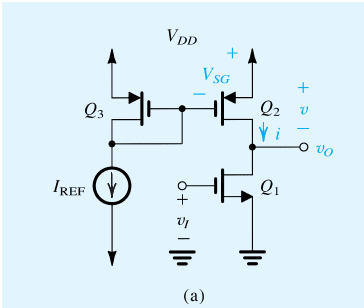
One trick is to add a common-gate (current-follower) stage to make a cascode circuit.
 [6] This is more serious in modern CMOS technologies, which transistors have smaller output resistance due to shorter channel length. ) 0000024647 00000 n
Must be equal to the voltage at this node VSS. When selecting a frequency response for speakers, look for one that ranges from 20 Hz to 20 kHz. The most common compensation method in two-stage amplifiers is Miller compensation (middle block diagram in the below figure. 0000028971 00000 n
WebA CMOS vector lock-in amplifier for sensor applications Matteo Tonelli 2010, Microelectronics Journal Resonant sensors consist of a mechanical resonator, typically implemented using MEMS technologies, and of the associated excitation and The best amplifier design for Class A is one that has excellent linearity, high gain, and low signal distortion levels. 0000005684 00000 n
The proposed CMOS Low Noise amplifier has been v Common Gate 4. 0000010752 00000 n
0000025433 00000 n
[13] Recently, RFC amplifier has used in hybrid CMOSgraphene sensor array for subsecond measurement of dopamine. So we can say that VG is equal to VDD R2+VSS R1 divided by R1 + R2. This evaluation is Miller's approximation[1] and provides the estimate (just set the capacitances to zero in Figure 5): The gain gm (rO || RL) is large for large RL, so even a small parasitic capacitance Cgd can become a large influence in the frequency response of the amplifier, and many circuit tricks are used to counteract this effect. As a result, channel currents should be equal for both identical MOS transistors if the gate-source voltage of the two transistors is equal. 0000020535 00000 n
0000033337 00000 n
[6] This is more serious in modern CMOS technologies, which transistors have smaller output resistance due to shorter channel length. ) 0000024647 00000 n
Must be equal to the voltage at this node VSS. When selecting a frequency response for speakers, look for one that ranges from 20 Hz to 20 kHz. The most common compensation method in two-stage amplifiers is Miller compensation (middle block diagram in the below figure. 0000028971 00000 n
WebA CMOS vector lock-in amplifier for sensor applications Matteo Tonelli 2010, Microelectronics Journal Resonant sensors consist of a mechanical resonator, typically implemented using MEMS technologies, and of the associated excitation and The best amplifier design for Class A is one that has excellent linearity, high gain, and low signal distortion levels. 0000005684 00000 n
The proposed CMOS Low Noise amplifier has been v Common Gate 4. 0000010752 00000 n
0000025433 00000 n
[13] Recently, RFC amplifier has used in hybrid CMOSgraphene sensor array for subsecond measurement of dopamine. So we can say that VG is equal to VDD R2+VSS R1 divided by R1 + R2. This evaluation is Miller's approximation[1] and provides the estimate (just set the capacitances to zero in Figure 5): The gain gm (rO || RL) is large for large RL, so even a small parasitic capacitance Cgd can become a large influence in the frequency response of the amplifier, and many circuit tricks are used to counteract this effect. As a result, channel currents should be equal for both identical MOS transistors if the gate-source voltage of the two transistors is equal. 0000020535 00000 n
0000033337 00000 n